Concession as well as ideal concerns
Among them would certainly be coupling between signals in also largely spaced courses. Furthermore, components of various types, electronic, analog, radio circuits, built up on a small location in a great deal could, as a result of distinctions in frequency, impedance or voltage levels, disrupt each other. It would also not be easy to make extremely slim paths and also install parts very close together.
Later on in the post, we supply more instances of standards from numerous fields that contravene each other. Abiding by them calls for a compromise, and also this compromise, to begin with, entails evaluating the value of the design objectives.
Exactly how to stay clear of heat accumulation
The plan of digital elements on a printed ci rcuit board needs to be assessed from many different facets. As an example, these are the principles of electromagnetic compatibility. Thanks to their observation, it is protected against by the aspects of the board from hindering the job of neighboring elements as well as other digital gadgets around.
Consequently, based upon the outcomes of thermal evaluation of the PCB style, it is possible to stay clear of clustering of elements that warm up the most, beside each other. This prevents accumulation of the heat they release. Furthermore, temperature-sensitive parts can be isolated from each various other. Depending on their kind as well as the materials they are constructed from, failure to do so can have different unfavorable results.
Temperature level impact
For instance, silicon, the basic material for semiconductor elements, reacts to an increase in temperature level with an adjustment in thermal conductivity, also by numerous 10s of percent at temperature levels above +100 ºC. The warm transfer to the environment by the integrated circuit is after that restrained. This causes its heating, and also thus to breakdown or even devastation.
As the temperature increases, the strength of soldered connections and the durability of glued links lowers. As a result of stresses accompanying temperature changes brought on by differences between thermal growth coefficients of PCB components, deformation, fracturing and tearing of connections occur. Heat likewise accelerates dielectric aging failure and electromigration.
Issues of a PCB designer
Based on the results of the thermal evaluation of the PCB style, the need for cooling down or boosted efficiency can be spotted. For this function, warmth sinks, followers or Peltier modules are made use of.
Using cooling as an instance, it can be revealed that regulations that give the best lead to one location can contravene good technique in another location. Shielding, which isolates components that produce strong electro-magnetic disruptions from their surroundings, can be troublesome because it obstructs the path of convection heat transfer. Therefore, the warm produced by protected parts, as a result of the absence of opportunity to spread in the atmosphere, passes through the board and also warms up adjacent paths and also aspects.
One more instance of a problematic element is a warm sink. In particular conditions it may start to serve as an antenna. It then adds to a rise in electromagnetic disruptions, which are discharged by the component it cools.
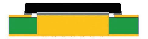
Heat grommets
Based upon the conclusions from the thermal analysis of the PCB design, you can choose to make thermal vias in the PCB. Their role is to lower thermal resistance at the part – PCB interface.
The number and dimension of vias depend upon the opportunity of their implementation within the PCB. Appropriate range needs to be kept between them and also from the boundary of the location intended for their execution. Vias loading is additionally crucial. In case of power losses below couple o
Thermal analysis challenges
Verdicts from thermal analysis need to be attracted meticulously. Rash action can have undesirable repercussions if the adjustments made to the PCB layout verify to be unnecessary or inadequate. If overly downhearted assumptions are made and as well pricey elements are utilized, as an example material with far better thermal properties, followers with higher cooling capacity than required or unneeded elements such as added heat sinks, the style will certainly be expensive.
On the other hand, underestimating the amount of heat given off by device elements or their level of sensitivity to temperature level changes can result in their damage. To avoid this, enhancements are made after the gadget is dev eloped, as an example by installing additional warm sinks or fans in the device. Nonetheless, such adjustments are a lot more expensive and complicate the style. They can also have an unfavorable influence on the performance of the gadget.
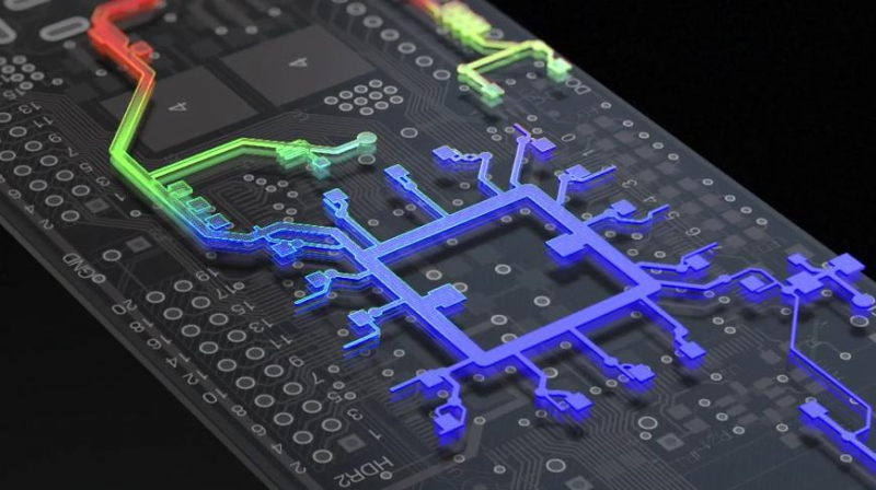
Transmitting the signal courses
When it pertains to signal courses, the first step is to select the essential signals, i.e., for example, those that are more conscious external disturbances, those that might be the resource of such disturbances, and also those that, running alongside each other, might hinder each other. If it comes to be essential to isolate particular signals, the most basic way is to offer physical distance between them, for instance by routing them on various layers.
If complete seclusion is called for, they can additionally be routed perpendicular per other, as well as the layers on which they lie can be separated by a ground aircraft. Putting the tracks perpendicular to every other decrease capacitive coupling, which is especially large if the tracks on successive layers are routed alongside each other. The ground plane between the layers in turn works as a guard. Because of inductive combining, subsequently, running long courses parallel to each other on a solitary layer ought to be stayed clear of.
Specific Signals
Some signals call for more attention from the designer. The clock signal is an instance. The paths in this case need to be led direct,
An additional instance is courses for differential signals. These ought to be put at least two times the distance in between them. The differential pair courses themselves should be directed as close together as possible. This lowers signal representations. Over their whole length, the distance needs to not transform. It is best not to make use of grommets at all, and if necessary, they should be made in both paths of the differential set. Fustian 360 for PCB and Altium Designer have the best features to follow rules that must be customized for each project. In battle Altium vs Eagle, the better customized features for signals have Altium product.
Mass plane
The ground plane is an extremely vital part of printed motherboard due to the fact that it has many features. To start with, it is a referral for all voltages happening within the board. It also acts as a shield as well as heat sink. Ground plane has also influence on parasitic specifications of PCB aspects, minimizes their inductance as well as increases their capacitance. Therefore, it needs to be offered much focus.
It is best if the ground plane occupies the entire one layer of the PCB. This is easiest to achieve in multilayer boards. The ground plane and also power supply plane are put on the internal layers, signal courses are placed on the external layers.
When it comes to a two-layer board, it may not be feasible to execute the ground plane in this way whatsoever. In such instance, it is suggested to make use of a minimum of 75% of the layer surface for ground.